e2v EV10AS150A Bedienungsanleitung

ADC EV10AS150A Evaluation Board
User Guide

2ADC EV10AS150A User Guide
0977B–BDC–09/09

EV10AS150A-EB User Guide 1
0977B–BDC–10/09
Table of Contents
Section 1
Introduction ........................................................................................... 1-1
1.1 Scope1-1
1.2 Description ................................................................................................1-1
Section 2
Hardware Description ........................................................................... 2-1
2.1 Board Structure.........................................................................................2-1
2.2 Analog Inputs/Clock Input .........................................................................2-2
2.3 Digital Output ............................................................................................2-3
2.4 Reset Lines ...............................................................................................2-5
Section 3
Operating Characteristics ..................................................................... 3-1
3.1 Introduction ...............................................................................................3-1
3.2 Operating Procedure.................................................................................3-1
3.3 Electrical Characteristics...........................................................................3-2
3.4 Digital Output Coding................................................................................3-4
Section 4
Software Tools...................................................................................... 4-1
4.1 Overview ...................................................................................................4-1
4.2 Configuration.............................................................................................4-1
4.3 Getting Started..........................................................................................4-1
4.4 Operating Modes ......................................................................................4-7
Section 5
Application Information ......................................................................... 5-1
5.1 Introduction ...............................................................................................5-1
5.2 Analog Inputs ............................................................................................5-1
5.3 Clock Inputs ..............................................................................................5-1
5.4 Digital Outputs ..........................................................................................5-1
5.5 ADC Functions..........................................................................................5-2
5.6 DMUX Functions .......................................................................................5-2
5.7 Diode for Die Junction Temperature Monitoring .......................................5-4
5.8 Test Bench Description.............................................................................5-6
Section 6
Package Information............................................................................. 6-1
6.1 Thermal Characteristics ............................................................................6-1

2EV10AS150A-EB User Guide
0977B–BDC–10/09
Section 7
Ordering Information............................................................................. 7-1
Section 8
Appendix............................................................................................... 8-1
8.1 EV10AS150A-EB Electrical Schematics ...................................................8-1
8.2 EV10AS150A-EB Board Layers................................................................8-9

EV10AS150A-EB User Guide 1-1
0977B–BDC–10/09
e2v semiconductors SAS 2009
Section 1
Introduction
1.1 Scope The ADC EV10AS150A-EB Evaluation Kit is designed to facilitate the evaluation and
characterization of the different versions of EV10AS150A ADC with 1:2/4 DMUX up to
its 5 GHz full power input bandwidth.
The ADC EV10AS150A-EB Evaluation Kit includes:
The EV10AS150A with 1:2/4 DMUX Evaluation board including one version of the
EV10AS150A ADC device soldered on the board
Six SMA caps for CLK, CLKN, VIN, VINN, DRR and ASYNCRST signals
Six jumpers DMUX function settings (RS, BIST, DRTYPE, SLEEP, STAGG),
CLKTYPE jumper is not used
3-wire serial link to control ADC functionality
The user guide uses the EV10AS150A Evaluation Kit as an evaluation and demonstra-
tion platform and provides guidelines for its proper use.
1.2 Description The ADC EV10AS150A Evaluation board is very straightforward as it only implements
the EV10AS150A ADC/DMUX device, SMA connectors for the sampling clock, analog
inputs and reset inputs accesses and HE14 double row 2.54 mm pitch connectors com-
patible with high speed acquisition system probes.
To achieve optimal performance, the ADC EV10AS150A-EB Evaluation board was
designed in a 8-metal-layer board with RO4003 200 µm and FR4 HTG epoxy dielectric
materials. The board implements the following devices:
The ADC EV10AS150A with 1:2/4 DMUX Evaluation board with one version of the
EV10AS150A ADC soldered on the board
Six SMA caps for CLK, CLKN, VIN, VINN, DRR and ASYNCRST signals
Six jumpers DMUX function settings (RS, BIST, DRTYPE, SLEEP, STAGG),
CLKTYPE jumper is not used
3-wire serial link to control ADC functionality via RS232
2.54 mm pitch connectors for the digital outputs, compatible with high speed
acquisition system probes
Banana jacks for the power supply accesses and the die junction temperature
monitoring functions (2 mm)
Potentiometers for the DMUX functions

Introduction
1-2 EV10AS150A-EB User Guide
0977B–BDC–10/09 e2v semiconductors SAS 2009
The board is composed of eight metal layers for signal traces, ground and power supply
layers, and seven dielectric layers featuring low insertion loss and enhanced thermal
characteristics for operation in the high frequency domain.
The board dimensions are 220 mm x 240 mm.
The board comes fully assembled and tested, with one version of the EV10AS150A
ADC installed.
Figure 1-1. ADC EV10AS150A-EB Evaluation Board Simplified Schematic
As shown in Figure 1-1, different power supplies are required:
VCCA5 = 5.0V analog positive power supply
VCCA3 = 3.3V analog positive power supply
VCCD = 3.3V digital positive power supply
VPLUSD = 2.5V digital output power supply
3.3V power supply for the board functions
PIN 1
Port D
Port C
Port B
Port A
DMUX functions
VIN
VINN
CLKNCLK
ASYNCRST
DRR
Diode
CLKDACTRL
G
N
D
3
V
3
G
N
D
G
N
D
G
N
D
DR
ADC
EV10AS150A
G
N
D
V
C
C
A
3
3
V
3
V
C
C
A
5
5
v
2
V
C
C
D
3
v
3
V
+
D
2
V
5
DMUX functions
RS232

EV10AS150A-EB User Guide 2-1
0977B–BDC–10/09
e2v semiconductors SAS 2009
Section 2
Hardware Description
2.1 Board Structure
In order to achieve optimum full speed operation of the ADC EV10AS150A with 1:2/4
DMUX, a multilayer board structure was retained for the evaluation board. Eight copper
layers are used, respectively dedicated to the signal traces, ground planes, power sup-
ply planes and DC signals traces.
The board is made in RO4003 200 µm and FR4 HTG epoxy dielectric materials. Table
2-1 gives a detailed description of the board's structure.
Table 2-1. Board Layer Thickness Profile
Layer Characteristics
Layer 1
Copper layer
Copper thickness = 40 µm
AC signals traces = 50Ωmicrostrip lines
DC signals traces (DMUX functionality etc.)
Layer 2
RO4003 dielectric layer (Hydrocarbon/wovenglass)
Layer thickness = 200 µm
Dielectric constant = 3.4 at 10 GHz
–0.044 dB/inch insertion loss at 2.5 GHz
–0.318 dB/inch insertion loss at 18 GHz
Layer 3
Copper layer
Copper thickness = 35 µm
Upper ground plane = reference plane 50Ωmicrostrip return
Layer 4
FR4 HTG/dielectric layer Layer thickness = 170 µm
Layer 5
Copper layer
Copper thickness = 35 µm
Power planes = VCCA5
Layer 6
FR4 HTG/dielectric layer Layer thickness = 200 µm
Layer 7
Copper layer
Copper thickness = 35 µm
Power planes = VCCD and 3.3V
Layer 8
FR4 HTG/dielectric layer Layer thickness = 170 µm

Hardware Description
2-2 EV10AS150A-EB User Guide
0977B–BDC–10/09 e2v semiconductors SAS 2009
The board is 1.6 mm thick.
The clock, analog input, reset and digital data output signals occupy the top metal layer
while the ADC and DMUX functions are located both on the top.
The ground planes occupy layer 3, 13 and 15 (partly).
Layer 5, 7, 9 and 11 are dedicated to the power supplies.
2.2 Analog
Inputs/Clock
Input
The differential active inputs (Clock, Analog) are provided by SMA connectors.
Reference: VITELEC 142-0701-8511
Special care was taken for the routing of the analog input and clock input signals for
optimum performance in the high frequency domain:
50Ωlines matched to ±0.1 mm (in length) between VIN and VINN and between CLK
and CLKN
50 mm max line length
1.27 mm pitch between the differential traces
400 µm line width
40 µm thickness
850 µm diameter hole in the ground layer below the VIN, VINN, CLK and CLKN ball
footprints
Layer 9
Copper layer
Copper thickness = 35 µm
Power planes = VCCA3
Layer 10
FR4 HTG/dielectric layer Layer thickness = 200 µm
Layer 11
Copper layer
Copper thickness = 35 µm
Power planes = VPLUSD
Layer 12
FR4 HTG/dielectric layer Layer thickness = 170 µm
Layer 13
Copper layer
Copper thickness = 35 µm
Ground plane = reference plane (identical to layer 3)
Layer 14
FR4 HTG/dielectric layer Layer thickness = 200 µm
Layer 15
Copper layer
Copper thickness = 40 µm
DC signals traces and Serial Interface (AVR) signals
Ground plane
Table 2-1. Board Layer Thickness Profile (Continued)

Hardware Description
EV10AS150A-EB User Guide 2-3
0977B–BDC–10/09
e2v semiconductors SAS 2009
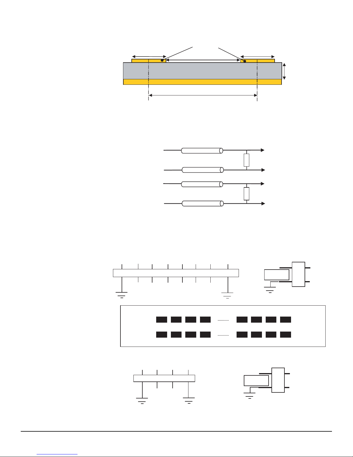
Figure 2-1. Figure 2-1.Board Layout for the Differential Analog and Clock Inputs
Figure 2-2. Differential Analog Inputs Implementation
Figure 2-3. Differential Clock Inputs Implementation
2.3 Digital Output The digital output lines were designed with the following recommendations:
50Ωlines matched to ±0.5 mm (in length) between signal of the same differential pair
80 mm max line length
±1 mm line length difference between signals of two ports
±1.5 mm max line length difference between all signals
770 µm pitch between the differential traces
370 µm line width
40 µm thickness
200
µ
m
RO4003
400 µm 400
µm
870
µm
µ1270 m
e= 40µm
Ground plane
VIN (H27)
VINN (J27)
VIN
VINN
100 pF
100 pF
EV10AS150A
100 pF
CLK
CLKN
CLK (W23)
CLKN (RW24)
100 pF
EV10AS150A

Hardware Description
2-4 EV10AS150A-EB User Guide
0977B–BDC–10/09 e2v semiconductors SAS 2009
Figure 2-4. Board Layout for the Differential Digital Outputs
The digital outputs are compatible with LVDS standard. They are on-board 100Ωdiffer-
entially terminated as described in Figure 2-5.
Figure 2-5. Differential digital Outputs Implementation
HE14 Double row 2.54 mm pitch connectors are used for the digital output data. The
upper row is connected to the signal while the lower row is connected to Ground, as
illustrated in Figure 2-6.
Figure 2-6. Differential Digital Outputs 2.54 mm Pitch Connector (Example Port A)
Figure 2-7. Differential Digital Clock Outputs 2.54 Mm Pitch Connector
200 µm
RO4003
3
7
0
µ
m
370µm
400 µm
770 µm
e= 40µm
Ground Plane
Di
DiN
100Ω
50Ω
Line
50Ω
Line
DRN
DR
100Ω
50Ω
Line
50Ω
Line
A0N A0 AORN
/DRA
AOR
/DRAN
…
Ground
Signal
GND A0N A0 A1N AORN AOR GND B0
GND GND GND GND GND GND GND GND
DR DRN
Signal
Ground
Inhaltsverzeichnis
Andere e2v Hauptplatine Handbücher

e2v
e2v EV8AQ160 Bedienungsanleitung

e2v
e2v AT84CS001-EB Bedienungsanleitung

e2v
e2v TSEV81102G0FS Bedienungsanleitung

e2v
e2v AT84AS003-EB Bedienungsanleitung

e2v
e2v EV8AQ160-EB Bedienungsanleitung

e2v
e2v TSEV8308500 Bedienungsanleitung

e2v
e2v TSEV8388B Bedienungsanleitung

e2v
e2v EV10AQ190-EB Bedienungsanleitung
Beliebte Hauptplatine Handbücher anderer Marken

Telit Wireless Solutions
Telit Wireless Solutions SL869-3DR Bedienungsanleitung

Gigabyte
Gigabyte GA-9IVDT Bedienungsanleitung

Texas Instruments
Texas Instruments ADS8372EVM Bedienungsanleitung

Commell
Commell MS-C73 Bedienungsanleitung

IBT Technologies
IBT Technologies MB860 Bedienungsanleitung

Nvidia
Nvidia TEGRA DG-04927-001_V01 Bedienungsanleitung