TB-7VX-690T/980T/1140T-PCIEXP Hardware User’s Manual
4
List of Figures
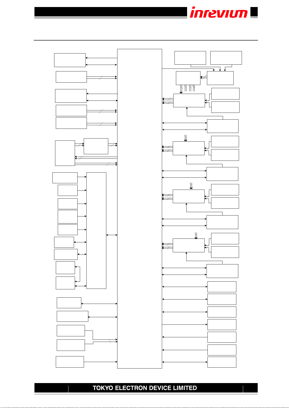
Figure 4-1 Block Diagram .................................................................................................................. 9
Figure 5-1 Component Side of the Board ........................................................................................ 10
Figure 6-1 Board Dimension Diagram...............................................................................................11
Figure 7-1 Power Supply Structure.................................................................................................. 12
Figure 7-2 Clock Structure ............................................................................................................... 13
Figure 7-3 Programable Clock Connection...................................................................................... 15
Figure 7-4 Connection of clock switch ............................................................................................. 16
Figure 7-5 High-Pin Count Pin Layout ............................................................................................. 17
Figure 7-6 DIMM1 and DIMM2......................................................................................................... 42
Figure 7-7 QSPI Layout ................................................................................................................... 52
Figure 7-8 LED Layout..................................................................................................................... 54
Figure 7-9 GPIO Pin Layout............................................................................................................. 55
Figure 7-10 DIPSW Structure........................................................................................................... 56
Figure 7-11 PUSHSW Structure....................................................................................................... 57
Figure 7-12 Power Connector for FAN............................................................................................. 58
Figure 7-13 Battery........................................................................................................................... 58
Figure 7-14 XADC Structure ............................................................................................................ 59
Figure 9-1 location of SW and CN(Juspmer)................................................................................... 60
List of Tables
Table 7-1 Details of Onboard Oscillator ........................................................................................... 14
Table 7-2 Clock Selection................................................................................................................. 16
Table 7-3 FMC1 Connector Pinout................................................................................................... 18
Table 7-4 FMC2 Connector Pinout................................................................................................... 24
Table 7-5 FMC3 Connector Pinout................................................................................................... 30
Table 7-6 FMC4 Connector Pinout................................................................................................... 36
Table 7-7 DDR3 SO-DIMM-1 Pinout................................................................................................ 43
Table 7-8 DDR3 SO-DIMM-2 Pinout Table....................................................................................... 46
Table 7-9 PCI Express Edge Pinout Table....................................................................................... 49
Table 7-10 PCI Express Lane Width Configuration.......................................................................... 50
Table 7-11 PMOD Pinout Table........................................................................................................ 51
Table 7-12 QSPI Pinout Table.......................................................................................................... 52
Table 7-13 USB3.0 Pin Assign......................................................................................................... 53
Table 7-14 LED Pinout Table............................................................................................................ 54
Table 7-15 GPIO Pinout Table.......................................................................................................... 55
Table 7-16 DIPSW Pinout Table....................................................................................................... 56
Table 7-17 PUSHSW Pinout ............................................................................................................ 57
Table 7-18 External Power Supply Connector Pinout Table ............................................................ 58
Table 7-19 Battery Control signal Pinout Table................................................................................ 58
Table 7-20 XADC Pinout Table......................................................................................................... 59
Table 9-1 Initial Settings................................................................................................................... 60