Freescale Semiconductor TWR-MPC5125 Bedienungsanleitung

TWR-MPC5125
User Manual
semiconductor

Table of Contents
01
TWR-MPC 5125
TWR-MPC5125 User Manual Made by
www. .com
semiconductor
1.0 General Description
2.0 Hardware Design & Architecture
3.0 Control & Configuration
4.0 Schematic
Operation
6.0 U-boot, Linux setup
7.0 How to build U-Boot, Kernel and device-tree
8.0 How to program NAND
Appendix A
Appendix B
5.0
1.1
2.1 General Description
2.2 Physical Specifications
2.3 Debugger Interface
2.4 Physical Specifications
3.1 Switch Settings
3.2 Sw7 – Power On Reset
3.3 Sw1 – Boot Mode
3.4 Configuration Header Settings
5.1 Central Processing Unit
5.2 Power supplies
5.3 Resets
5.4 Memory
6.1 Host Computer Setup
6.2 Target Setup
6.3 Configuring U-Boot
6.4 NFS Root Development Deployment
6.5 How to boot from net_ramboot
7.1 Cross-compilation settings
7.2 How to build
8.1 Program Loader and U-boot
8.2 Program Device-tree and Kernel
8.3 Upgrade Filesystem from the U-Disk
--Connector Pin Assignments
--Memory Map
Device Placement and Functions
02
02
07
07
07
07
08
09
09
09
09
10
11
12
12
12
12
13
14
14
15
16
19
19
21
21
21
23
23
26
26
28
29
S / N : MP C 5 1 2 5 1 0 0 3 0 0 0 1
DC 5V
TWR-MPC5125 User Manual Made by
www. .com
semiconductor
1.0 General Description
1.1 Device Placement and Functions
02
TWR-MPC 5125
The MPC5125 Tower System is based on Freescale's MPC5125
microprocessor. The board provides on-board DDR2 SDRAM, NAND
FLASH,CAN ports, USB 2.0, 10/100 Ethernet, HDMI,USB Debug Port.All
powered from a 5 Volt wall mount power supply.
Freescale's Tower System. For information of Tower System, please go to
http://www.freescale.com/tower .
This board is compatible with
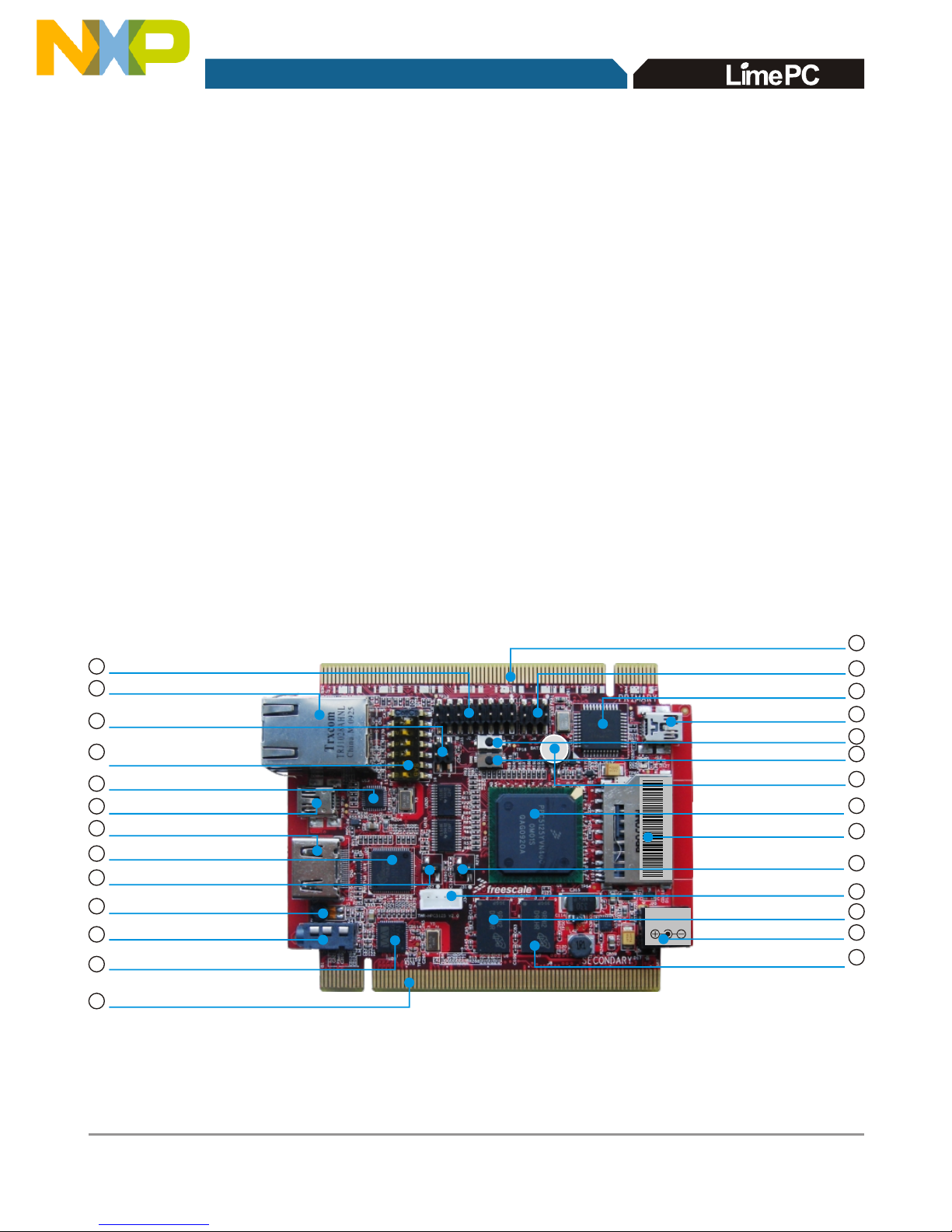
This section provides a description of the connectors, jumpers, switches and
main components of the MPC5125 board. Refer to Figures 1 and 2 for
location of the devices referenced below.
SW1 System
Config Switch
CN1 RJ45 Ethernet Connector
J33 Depopulated
Battery Site
Mini-AB USB Connector
U13 USB PHY
CN3 HDMI Connector
U20 HMDI Transmitter
J2 JTAG Connector
Primary Elevator connector
U14 Debug MCU
J19 USB Debug port
J20 DC In
J4 Debug MCU Config Header
U1 MPC5125
Secondary Elevator Connctor
SW7 Reset Swich
U6 DDR Memory
U7 DDR Memory
Figure 1
SD Card Connector
SW8 Hibemate Swich
J1 Earphone Connector
U28 Audio CODEC
J3 On-Board Microphone (MIC)
2
4
5
6
7
8
10
12
13
14
15
16
17
18
19
20
21
22
26
25
27
1
J35 Serial Port Header
3
J27 Dual-Ethernet Jumper
9
11
J31 CAN Termination
Jumper 23
24
J34 CAN Connector

MAC:00-22-78-00-49-7A
TWR-MPC5125 User Manual Made by
www. .com
semiconductor
03
TWR-MPC 5125
Additional descriptions of the functionality of switches and jumpers along with
their recommended settings can be found in Section 3 of this manual.
1
U2 Ethernet PHY
U10 NAND Flash Memory
28
30
Figure 2
J2- JTAG Connector
Connector J2 is a 16-pin header used for the COP/JTAG input. This port is
made available to aid of debugging code running on the MPC5125.The pin-
outs for the connector are listed in Appendix A
29 U4 Digital Accelerometer

2
3
Cn1 RJ45 Ethernet Connector
Cn1 is a standard Ethernet input jack
J35 Serial Port Header
J35 is the serial port header with the following 2x2 header to MPC5125 pin
assignments:
7
8
9
4
5
6
SW1 System config switch
See switch settings. Section 3
U13 USB PHY
U13 is a Hi-Speed USB 2.0 ULPI transceiver
Mini-AB USB Connector
DOWN4 is a USB mini AB connector that is compatible with the USB 2.0
format.
CN3 HDMI Connector
CN3 is a HDMI interface
U20 HMDI Transmitter
U20 is a HDMI transmitter
J27 Dual-Ethernet Jumper
J27 is the dual-Ethernet jumper. Connecting a jumper across the terminals
will enable a second Ethernet connection to be made over the Primary
Elevator Connector in addition to the CN1 RJ45 Ethernet jack. Connecting
this jumper will disable the Mini-AB USB Connector.
TWR-MPC5125 User Manual Made by
www. .com
semiconductor
04
TWR-MPC 5125
PSC2_2
PSC2_3
PSC2_0
PSC2_1

J3 On-Board Microphone (MIC)
Audio input
J1 Earphone Connector
Audio output
U28 Audio CODEC
U28 is Audio CODEC
Secondary Elevator Connctor
Secondary Elevator Edge Connector for the Freescale TOWER system
Primary Elevator connector
Primary Elevator Edge Connector for the Freescale TOWER system
J4 Debug MCU Config Header
See section 3.4 for configuration header settings. A BDM module can be
connected as shown to debug code running on the Debug MCU.
U14 Debug MCU
U14 is Debug MCU which performs the USB to MPC5125 debug bridge
from the USB Debug Port.
J19 USB Debug port
J19 is the USB Debug port for the MPC5125. Power can be provided to
the system over this USB port.
SW7 Reset switch
SW7 is a Hardware Reset switch. Push once causes a Power on reset.
TWR-MPC5125 User Manual Made by
www. .com
semiconductor
10
11
12
13
14
15
16
17
18
05
TWR-MPC 5125
Pin 2
Pin 4
Pin 6
Pin 1
Pin 3
Pin 5

06
TWR-MPC 5125
TWR-MPC5125 User Manual Made by
www. .com
semiconductor
SW8 Hibernate Switch
SW8 is hibernate switch
Push it to wake up the system
J33 Depopulated Battery Site
Location to add a battery or capacitor for the Real Time Clock VBAT_RTC
power domain.Recommended capacitor is EECEN0F204RT from
Panasonic .
U1 MPC5125
U1 is Freescale's MPC5125 microprocessor
SD Card Connector
SD card interface
J31 CAN Termination Jumper
J31 is the CAN jumper location. Connecting a jumper across the terminals
will add termination to the CAN interface which is normally not terminated.
J34 CAN Connector
J34 is a CAN connector
U6 DDR Memory
U6 is DDR2 Memory for system running
J20 DC IN
J20 is the 5V DC input to the board
U7 DDR Memory
U7 is DDR2 Memory for system running
U10 NAND Flash Memory
U10 is a NAND Flash for uboot, Linux kernel, file system and user data
U4 Digital Accelerometer
U4 is a digital accelerometer
U2 Ethernet PHY
U2 is the Ethernet PHY with MII/RMII interface.
20
21
22
23
24
25
26
27
28
29
DC 5V
19
30

2.0 Hardware Design & Architecture
2.1 Memory
07
TWR-MPC 5125
4GB MLC NAND flash storage
256MB DDR2 memory
TWR-MPC5125 User Manual Made by
www. .com
semiconductor
Digital accelerometer
- HDMI(video/audio) port with HDMI to DVI--D adaptor
- RJ-45 10/100 Base T Ethernet port
Mini-AB USB2.0 OTG
USB host to hub (keyboard, mouse, sound , card, WiFi,....)
USB device to external USB host system
On-board microphone and audio stereo out jack
SD Card expansion port
CAN2.0 A/B port
-
-
-
-
2.2 Connectving & Features
On-board debugger over Mini-B USB port
JTAG/COP header for external BDM
2.3 Debugger Interface

2.4 Physical Specifications
08
TWR-MPC 5125
This section contains general information on the MPC5125's physical
characteristics
Board Size: Freescale Tower specification(59mm x 90mm)
Power Requirement: 5VDC
Operating Temperature: 0℃ to +70℃
Weight: 50g
RoHS: Compliant
FCC/CE: Compliant
TWR-MPC5125 User Manual Made by
www. .com
semiconductor
EMB_AD[0:31]
DDRⅡ CONTROLLER AND DATA
BUS @200MHz,(DDR2-400)
12C /1
JATG
USB Debug Port
Serial Header
LAN PHY

3.0 Control & Configuration
3.1 Switch Settings
09
TWR-MPC 5125
This section contains general set-up information about the various jumpers,
switches on the MPC5125 board.
This section provides a brief description of the functionality and recommended
settings for the switches located on the MPC5125
Refer to Figure 1 for the locations of these switches.
3.2 Sw7 – Power On Reset
Sw7 is a push button that provides a power on reset signal for the hardware
on the MPC5125.
3.3 Sw1 – Boot Mode
The mode switch provides configure the different operation of the MPC5125.
TWR-MPC5125 User Manual Made by
www. .com
semiconductor
SW1 Position Reset Configuration Signal Description Default
6 RST_CONF_ROMLOC0 Boot Device Select
0 = LPC Boot, 1 = NAND (NFC) boot 1
5 RST_CONF_BMS Boot Mode Select
0 = boot low, 1 = boot high 1
4 RST_CONF_LPC_DBW0 LPC Data Port Size
3 RST_CONF_LPC_DBW1 00 = 8-bit, 01 = 16-bit, 10 = reserved, 11 = 32-bit 00
2 RST_CONF_LPCWA LPC Word/Byte Address Mode
0 = word address mode, 1 = byte address mode 1
1 RST_CONF_LPCMX LPC Multiplex Mode
0 = non-multiplexed mode, 1 = multiplexed mode 0
Andere Handbücher für TWR-MPC5125
1
Inhaltsverzeichnis
Andere Freescale Semiconductor Desktop Handbücher


